Though this is not strictly Apple II related, since the Altera Max 7000 series CPLD is popular here, I feel I have a duty to warn.
I can't find the exact quote from UncleBernie, but I remember reading him telling about "in his days" people having their expectations about CPLD/FPGA being 'reajusted' by reality. The last couple of days have been such days for me.
I have been fixing/annoyed by/cursing at an issue with the AUX RAM / Motherboard RAM, where it seemed fixing one would break the other. To be precise, an issue with the enabling of the address bus by the IOU/MMU.
Let me first write a little refresher on what happens in the MMU / IOU for those unfamiliar or have forgotten how it works:
The RA bus on the Apple IIe is the multiplexed address bus and it is shared between the MMU and the IOU; the MMU drives the bus when PHI_0 is HIGH, and the IOU drives it when PHI_0 is LOW. When the MMU or IOU is not driving the RA bus, it sets it to a high-impedance state. If we consider the MMU, it drives the bus from the rising edge of /RAS in the previous cycle to the falling edge of Q3 of the current cycle. However, a requirement of the RAM used in the Apple II serie is that the RA bus must hold it's value for some short delay past the falling edge of Q3. One way to do this (a.k.a the way I do it), when using an Altera device, is to use the LCELL primitive; it adds ~5 ns per LCELL and is useful when precise timing is not required.
The LCELL is a buffer and, besides the delay, should not modify the signal in any way. I have simplified the problem to this VHDL code:
In short: TEST_SIGNAL is computed from Q3 not-and PHI_0, and is connected to LCELL_DELAYED through a series of 10 LCELLs. One should expect LCELL_DELAYED to be the same as TEST_SIGNAL, delayed by ~50ns.
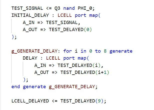
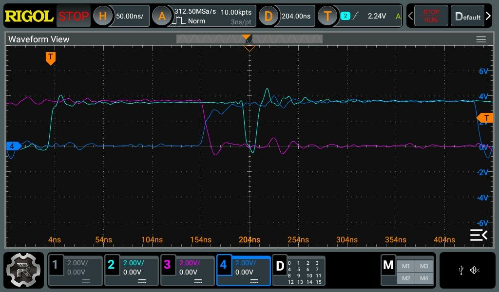
But that's not what we have:
Yellow is TEST_SIGNAL,
Cyan is LCELL_DELAYED,
Magenta is PHI_0,
Blue is Q3
I have not forgotten to turn off the setting to ignore LCELLs in Quartus; you can see the cyan signal is lagging the yellow one by ~50ns.
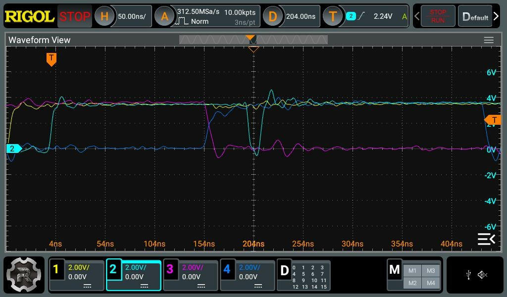
But the above image is a bit crowded, so let's look at just TEST_SIGNAL and LCELL_DELAYED:
You can see LCELL_DELAYED dropping but TEST_SIGNAL is not!
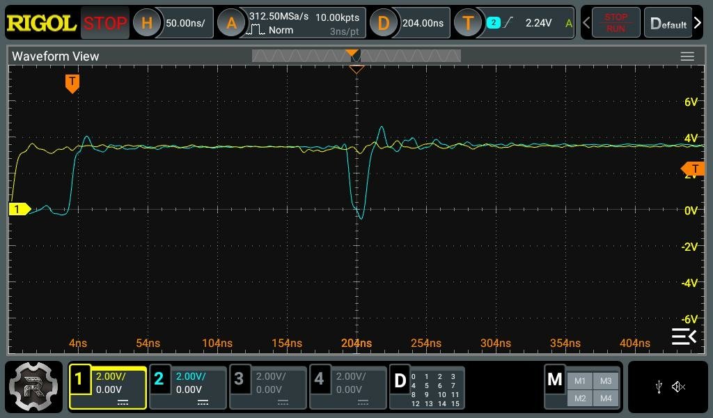
It's the LCELLs that are causing this drop; this is what a 2-LCELLs looks like:
The more LCELLs you add, the more severe the drop is.
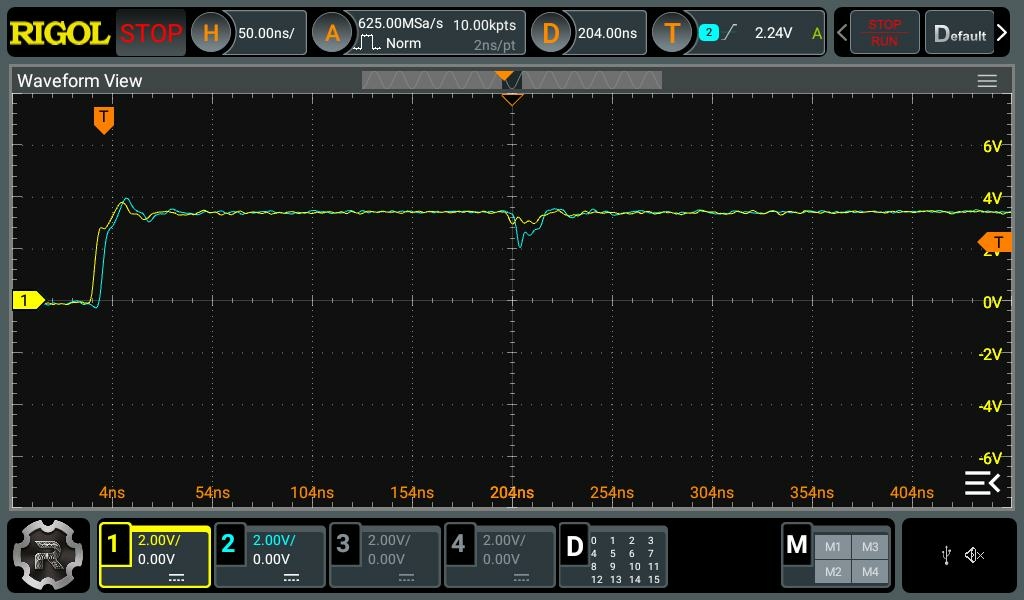
Normally, LCELLs behave as expected, but in the above case, I think it's due to the fact that TEST_SIGNAL is computed from a slow-changing signal (Q3):
As you can see the drop is ~50ns after the PHI_0 / Q3 change.
I am not finding anything on the internet about this. Maybe I just don't know what to google, but in any cases, it's something useful to be aware of.
Similar glitches I reported some time ago when inspecting my setup. I concluded the project has many more difficulties to overcome due to the different and obscured (by altera in this case) building bricks it uses. The circuit diagram on which MMU and IOU are based appears to be the smaller part of the task of emulating these devices with relatively contemporary technologies.
Uncle Bernie's take on this is:
DON'T USE THEM FOR MAKING EXTERNAL TIMING SIGNALS !
The reason behind this advice is based on the fact that when using CMOS, unlike bipolar (TTL, LSTTL...), there is no such thing as a defined delay. The delay of simple CMOS gates is all over the place, depending on process corner, power supply voltage, and die temperature. There are some trick circuits which can partially compensate for these effects over process, supply voltage, and temperature, but the simpler ones are lacking, and the more elaborate ones use sophisticated analog circuits which draw current all the time, which is unwanted in most CMOS applications: customers expect that with no clock applied, the CMOS IC only draws a little bit of leakage current. So in the end, a lot of CMOS ICs featuring internal oscillators (or delays) have large tolerance bands on the frequency (or delay) or use factory trim to a target (i.e. many Microchip PIC MPUs with internal oscillator store a factory trim value in their EEPROM and the software must use it to get the oscillator right, and all programmers must have extra code to preserve the trim value so it does not get lost).
I don't know what Altera did to guarantee delay parameters for that LCELL, but I'd not be surprised if they did nothing.
So the use of any such delay cells must be limited to certain scenarios where it is used to pad up some internal signal path with extra delay to compensate for delay on another signal path. Done right, this can help to avoid hazards and critical races. It will work (usually) because all the gate delays in the same CPLD / FPGA track over process, supply voltage, and temperature.
But for meeting any timing criteria dictated by the external world these internal delay cells should better be avoided. You should use an external clock, or a sequence of signals coming from an external clock, to derive required timing for the external system. If you don't have any suitable signals, then you need to get creative or just add an external RC which you can adjust in production. Note that despite it's just a simple resistor and capacitor, the timing delay you will get depends on even more parameters unknown to you, such as the exact trip point of the input circuit, and you may need to add hysteresis to avoid ringing. If you do such a RC delay in an industrial, mass produced design, it either must be uncritical (so no trim is ever needed) or sooner or later you will be fired for making lousy designs. But we need to be pragmatic for hobbyist projects like your MMU and IOU replacements. These will never be mass produced and it is perfectly OK to leave out a SMD resistor, measure which value would be needed to get the right timing, and then put in the right resistor by hand soldering. I had the same situation with the 74123 oneshot in my Apple-1 IC kits, each 74123 had to get hand selected R's and C's to arrive at the correct time delays. This cost me about 3-5 minutes per set of 74123 and its R's and C's. Note that it is impossible to guarantee proper timing of the 74123 as needed by the Apple-1 just by putting in unselected components, even if you would specify 2% R's and C's, because the 74123 itself has larger tolerances than allowed by the Apple-1 design. And with carbon composition resistors it's totally hopeless to hit the right timing anyways, unless pre-ageing, pre-soldering, and hand selection is used. So the Apple-1 is not a design which could have been produced in larger numbers. But for the 100-150 units the fledgling "Apple Computer Company" operating out of Woz' garage ever made, it was probably OK to hand tweak each one. And with your MMU and IOU substitutes, in all likelyhood, you also won't ever do larger production runs.
So using hand tweaked RC delays probably is OK for your application. A much cleaner solution would be to add one wire carrying the 14M clock signal to both the MMU and the IOU substitute drop-in carrier PCBs but then it would involve soldering one wire to an IC pin to put them into an Apple IIe or IIc. But believe me, ALL the insidious timing problems with the MMU and IOU would just go away if you had that 14M clock available. This, BTW, is the route I took with my own MMU and IOU substitute designs. Only the very first incarnation did not use 14M, it used some RC delays instead. I can do this without an extra wire because my solutions are not meant to drop into DIL-40 sockets on original Apple II motherboards.
Hope this helps to get your project back on track.
- Uncle Bernie
Slow rise time + no input shmitt triger + fast input response ( Altera delay is about 2-3 ns ) = issue like this .
I see many of this situation when i develoip my hardware .
I use too lcell ( or similar ) delay technics ( of course this is unacceptable ) and not have issue if input signal is with fast rise time .